取り扱い品目
(取り扱い品目)
用途:自動車部品、光通信、半導体関連、等
1.金属:SUS、コバール、50アロイ他切削、フライス加工
2.セラミック、チッカアルミ、SIC、細穴、フライス加工
3.石英、パイレックス等、フライス、細穴、フライス加工
4.精密プレス、鍛造プレス、モールド成形及びMIM
5.表面処理 Ni+Bメッキ、クロムメッキ 他
100μmピッチ対応超極細コンタクトプローブ(特許公開中0000000号)
Super fine contact probes for 100μm pitch
(用途)◆パッケージ基盤、フラットパネルディスプレー、半導体、ウエハ基盤
その他、あらゆるアプリケーションに利用可能。
(特徴)◆100μmピッチをチューブ付き両端可動コンタクトプローブ構造で実現
◆低バネ圧設計により、パターン上の打痕傷を軽減
◆メンテナンス性を重視したグローブ交換方式を採用
(Application) ◆For testing of IC substrate, Flat Panel Display,Wafer,
(Features) ◆The smallest double ended type contact probe in the world.
◆Guarantee very stabls and low contact resistance.
◆Low and controlled spring force can creat damaged free
environment to the PCB during testing contact probes can be
remobed one by one,enabling user to performe a maintenance
swifty.
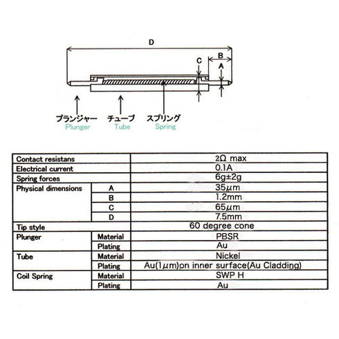
プローブ使用 Probe Specification